PCB Marking: Bare Board Identification
What Gets Marked on PCBs
Bare PCBs typically receive:
- Board serial numbers — Unique IDs for traceability
- Date codes — Manufacturing week/year
- Revision numbers — Design version tracking
- UL/CE certification marks — Compliance identification
- 2D DataMatrix codes — Machine-readable traceability
- Fiducial markers — Alignment reference points
The Challenge: Marking Without Damaging
Here’s the core tension: PCBs are fragile, multilayer structures. A bare FR4 board has copper traces, solder mask, silkscreen, and substrate layers. Hit it with too much laser energy, and you’ll:
- Burn through the solder mask, exposing copper traces
- Delaminate the substrate
- Create carbonized residue that affects electrical performance
- Mark on a copper trace instead of the silkscreen, causing a potential short
This is why UV lasers dominate PCB marking. The 355nm wavelength is absorbed by virtually all PCB materials (copper, FR4, solder mask, silkscreen) without the deep thermal penetration that fiber lasers cause.
UV Laser PCB Marking Parameters
| Parameter | Typical Range |
|---|---|
| Power | 3W–10W UV |
| Marking speed | 500–3,000 mm/s |
| Spot size | 15–50 μm |
| Depth | 5–30 μm (solder mask removal) |
| Marking area | 110 x 110 mm to 175 x 175 mm (F-theta dependent) |
The UV laser’s “cold marking” capability means it removes solder mask or ablates the silkscreen layer with minimal heat-affected zone (HAZ). The mark is clean, the surrounding material is undamaged, and the copper traces below remain intact.
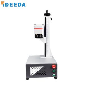
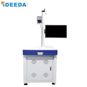
Looking for a UV laser system for PCB marking? [See our electronics marking solutions →]